- 您现在的位置:买卖IC网 > Sheet目录1233 > NCP1631PFCGEVB (ON Semiconductor)BOARD DEMO NCP1631 INTERLEAV PFC
�� �
�
�NCP1631�
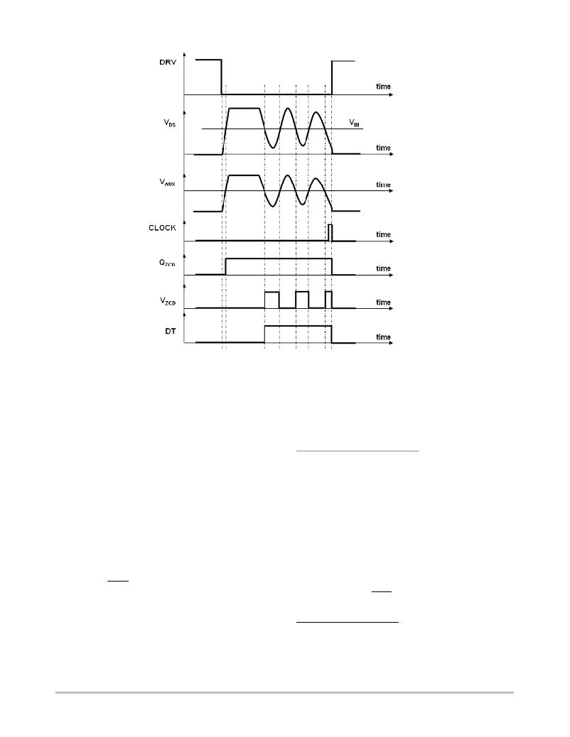
�Figure� 12.� Zero� Current� Detection� Timing� Diagram�
�(V� AUX� is� the� Voltage� Provided� by� the� ZCD� Winding)�
�R� CS�
�R� OCP� COIL�
�R� OCP�
�R� CS� ILIM1�
�Current� Sense�
�The� NCP1631� is� designed� to� monitor� a� negative� voltage�
�proportional� to� total� input� current,� i.e.,� the� current� drawn� by�
�the� two� interleaved� branches� (I� in� ).� As� portrayed� by�
�Figure� 13,� a� current� sense� resistor� (R� CS� )� is� practically�
�inserted� within� the� return� path� to� generate� a� negative�
�voltage� (V� CS� )� proportional� to� I� in� .� The� circuit� uses� V� CS� to�
�detect� when� I� in� exceeds� its� maximum� permissible� level.� To�
�do� so,� the� circuit� incorporates� an� operational� amplifier� that�
�sources� the� current� necessary� to� maintain� the� CS� pin�
�voltage� null� (refer� to� Figure� 13).� By� inserting� a� resistor�
�R� OCP� between� the� CS� pin� and� R� CS� ,� we� adjust� the� current�
�that� is� sourced� by� the� CS� pin� (I� CS� )� as� follows:�
�*� [R� CS� I� COIL� ]� )� [R� OCP� I� CS� ]� +� 0� (eq.� 10)�
�Which� leads� to:�
�I� CS� +� I� (eq.� 11)�
�In� other� words,� the� pin� 9� current� (I� CS� )� is� proportional� to�
�the� coil� current.�
�A� negative� clamp� protects� the� circuit� from� the� possible�
�negative� voltage� that� can� be� applied� to� the� pin.� This�
�protection� is� permanently� active� (even� if� the� circuit� off).�
�The� clamp� is� designed� to� sustain� 5� mA.� It� is� recommended�
�not� to� sink� more� than� 5� mA� from� the� CS� pin� for� a� proper�
�operation.�
�Two� functions� use� I� CS� :� the� over� current� protection� and�
�the� in� ?� rush� current� detection.�
�Over� ?� Current Protection (OCP)�
�If� I� CS� exceeds� I� ILIM1� (210� m� A� typical),� an� over� ?� current�
�is� detected� and� the� on� ?� time� is� decreased� proportionally� to�
�the� difference� between� the� sensed� current� I� IN� and� the�
�210� m� A� OCP� threshold.�
�The� on� ?� time� reduction� is� done� by� injecting� a� current� I� neg�
�in� the� negative� input� of� the� “V� TON� processing� circuit”�
�OPAMP.� (See� Figure� 7)�
�I� neg� +� 0.5(I� CS� *� 210� m� )� (eq.� 12)�
�This� current� is� injected� each� time� the� OCP� signal� is� high.�
�The� maximum� coil� current� is:�
�I� COIL(max)� +� I� (eq.� 13)�
�In� ?� rush Current Detection�
�When� the� PFC� stage� is� plugged� to� the� mains,� the� bulk�
�capacitor� is� abruptly� charged� to� the� line� voltage.� The�
�charge� current� (named� in� ?� rush� current)� can� be� very� huge�
�http://onsemi.com�
�13�
�发布紧急采购,3分钟左右您将得到回复。
相关PDF资料
NCP1650EVB
BOARD EVAL NCP1650 PFC CTLR
NCP1652L48VGEVB
BOARD EVAL 100W 48V NCP1652 PFC
NCP1653EVB
BOARD EVAL FOR NCP1653
NCP2993FCT2GEVB
BOARD EVAL NCP2993 AUDIO PWR AMP
NCP345SNT1G
IC DETECTOR OVER VOLTAGE 5TSOP
NCP346SN2T1G
IC DETECTOR OVER VOLTAGE 5TSOP
NCP347MTAITBG
IC OVERVOLTAGE PROT CTRLR 10WDFN
NCP348AEMUTBG
IC MOSFET DRIVER DUAL 12V 10LLGA
相关代理商/技术参数
NCP1650DR2
功能描述:功率因数校正 IC Fixed Frequency PFC RoHS:否 制造商:Fairchild Semiconductor 开关频率:300 KHz 最大功率耗散: 最大工作温度:+ 125 C 安装风格:SMD/SMT 封装 / 箱体:SOIC-8 封装:Reel
NCP1650DR2G
功能描述:功率因数校正 IC Fixed Frequency PFC PWM RoHS:否 制造商:Fairchild Semiconductor 开关频率:300 KHz 最大功率耗散: 最大工作温度:+ 125 C 安装风格:SMD/SMT 封装 / 箱体:SOIC-8 封装:Reel
NCP1650EVB
功能描述:电源管理IC开发工具 EVALUATION BOARD
RoHS:否 制造商:Maxim Integrated 产品:Evaluation Kits 类型:Battery Management 工具用于评估:MAX17710GB 输入电压: 输出电压:1.8 V
NCP1651DR2
功能描述:功率因数校正 IC Single Stage PFC RoHS:否 制造商:Fairchild Semiconductor 开关频率:300 KHz 最大功率耗散: 最大工作温度:+ 125 C 安装风格:SMD/SMT 封装 / 箱体:SOIC-8 封装:Reel
NCP1651DR2G
功能描述:功率因数校正 IC Single Stage PFC RoHS:否 制造商:Fairchild Semiconductor 开关频率:300 KHz 最大功率耗散: 最大工作温度:+ 125 C 安装风格:SMD/SMT 封装 / 箱体:SOIC-8 封装:Reel
NCP1652ADR2G
功能描述:功率因数校正 IC ANA PFC CONTROLLER RoHS:否 制造商:Fairchild Semiconductor 开关频率:300 KHz 最大功率耗散: 最大工作温度:+ 125 C 安装风格:SMD/SMT 封装 / 箱体:SOIC-8 封装:Reel
NCP1652DR2G
功能描述:功率因数校正 IC ANA PFC CONTROLLER RoHS:否 制造商:Fairchild Semiconductor 开关频率:300 KHz 最大功率耗散: 最大工作温度:+ 125 C 安装风格:SMD/SMT 封装 / 箱体:SOIC-8 封装:Reel
NCP1652DWR2G
功能描述:功率因数校正 IC ANA PFC CONTROLLER RoHS:否 制造商:Fairchild Semiconductor 开关频率:300 KHz 最大功率耗散: 最大工作温度:+ 125 C 安装风格:SMD/SMT 封装 / 箱体:SOIC-8 封装:Reel